
A polymer-assisted hybrid bonding platform that separates active and passive devices across vertically integrated wafers—enabling higher layout density, improved area efficiency, and scalable RF / EM / thermal co-design for next-generation MMICs
Why Conventional MMIC Layouts Are Reaching Their Limits

Passive networks dominate valuable epitaxial wafer area, limiting density, RF scalability, and thermal freedom
Conventional GaAs MMICs place active devices, passive components, matching networks, and interconnects on the same epitaxial wafer.
In many RF power amplifier designs, active devices occupy only a limited portion of the die, while passive networks such as capacitors, inductors, transmission lines, and routing structures dominate the layout footprint.
As RF systems demand higher integration density, broader bandwidth, and better thermal behavior, conventional 2D MMIC layouts are reaching their practical limits.
Go Beyond 2D MMIC
Separating active and passive functions across vertically integrated wafers creates a new design space for compact, high-density MMICs
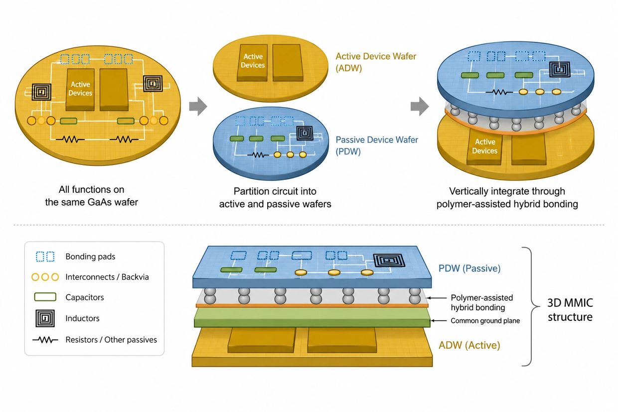
3DMMIC introduces a vertically integrated architecture that partitions RF circuits into two functional wafers.
Active transistors are fabricated on the Active Device Wafer, while passive networks, matching structures, transmission lines, and routing elements are implemented on the Passive Device Wafer.
The two wafers are integrated through polymer-assisted hybrid bonding, forming a compact 3D MMIC structure with improved layout density, better epitaxial resource utilization, and greater flexibility for RF / EM / thermal co-design.
Broadband PA Proof-of-Concept
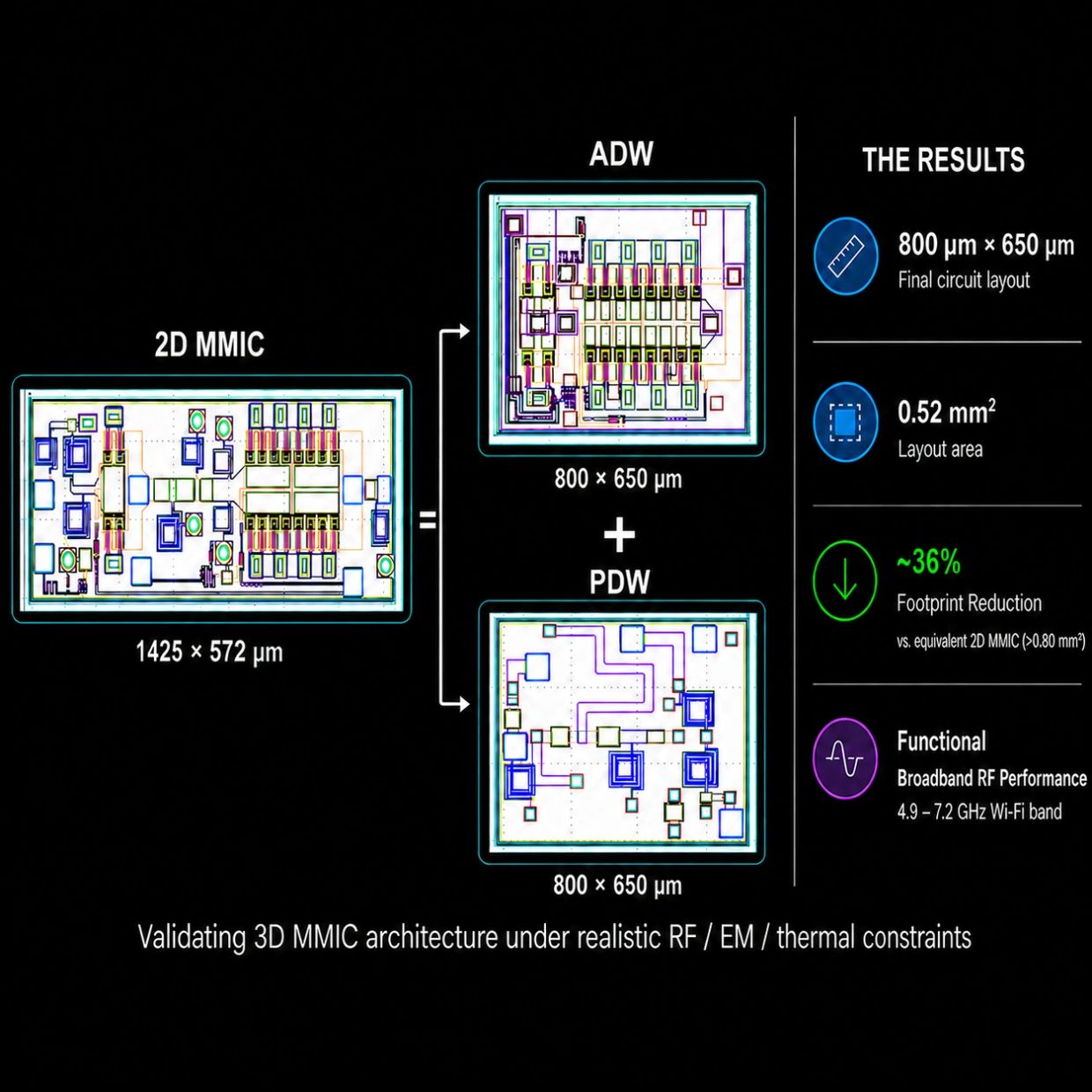
Illustration of the wafer-to-wafer Hybrid-bonded 3D MMIC Processes
This proof-of-concept compares a conventional 2D MMIC layout of 1425 × 572 μm with a hybrid-bonding 3D MMIC layout of 800 × 650 μm, demonstrating a 36% footprint reduction.
Manufactured with Standard Foundry Technology, Bonded with Commercial Tooling
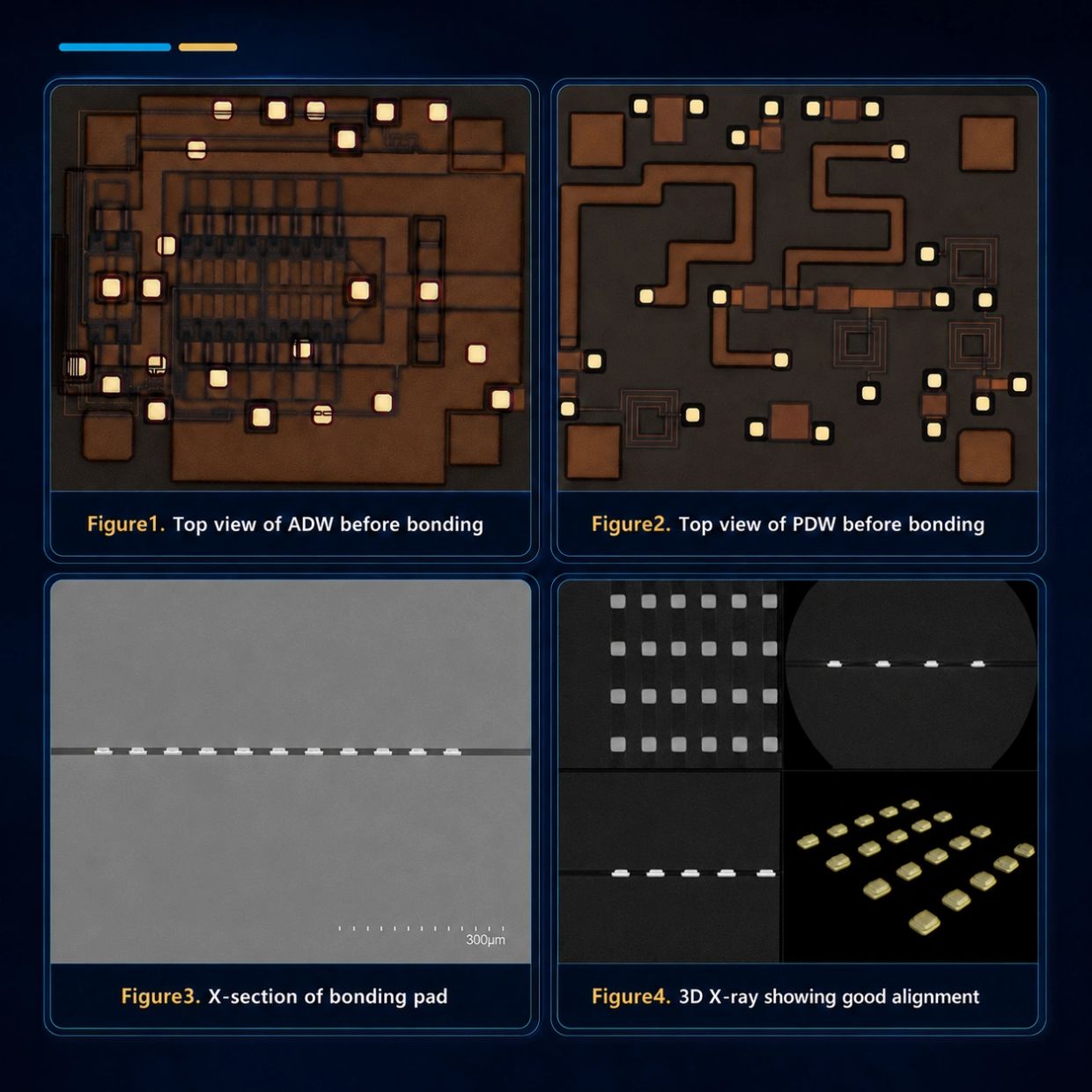
Process was done through low-temperature hybrid bonding experiments. By integrating Copper–Tin IMC bonding with dielectric polymer bonding, wafer-level 3D integration was demonstrated at 250 °C. SEM and 3D X-ray results confirmed uniform bump formation, interface alignment, and structural integrity, supporting the applicability of this process for RF 3D heterogeneous integration.